The circuit which is explained below is been employed as an Electronic
Letter Box. When letter drop by someone into the letter box then the
LED attached at the output stops blinking which indicates that there is a
letter in your letter box. To identify the presence of a letter in the
box we have connected a LDR as well as source of light. LDR is a special
kind of resistor whose action based on the intensity of light declining
on it. In the time of total darkness LDR resistance is approx 1 mega
ohm while at the time of bright light its resistance is 2-5 ohm. In this
circuit the light source is adjusted with the LDR in such a way that
the light will directly drop on the LDR so that when any letter comes
inside the letter box it will chunk the light beam and LDR will be
beneath darkness.
Electronic Letter Box Circuit Diagram:
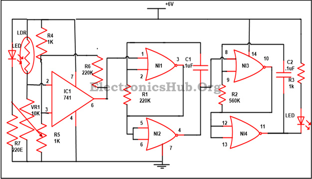
Circuit Diagram of Electronic Letter Box
Circuit Components:
- IC
- LM741 – 1
- CD4001 – 1
- Resistors
- R1(2.2M) – 1
- R2(560K) – 1
- R3,R4,R5(1K) – 3
- R6(220k) – 1
- R7(220E) – 1
- C1,C2(.1uF) – 2
- Miscellaneous
- LED1 – 2
- Vr1(10K) – 1
- LDR – 1
Component Description:
- LDR - It is a device whose sensitivity is based on the strength of the light incline on it. With the increase in the strength of the light, resistance of the LDR decreases and vice versa. When there is no light or in darkness, resistance of LDR reveal in the range of mega ohms while in the presence of light it move down to few hundred.
- LED - It consists of semiconductor which produces various colours of light as its output. LED produces narrow-spectrum light at the time it is electrically biased in the p-n junction at the forward bias state. When it is in the on mode, combines the electrons with holes and in the form of light energy releases.
- LM741 - It is basically all-purpose operational amplifier which is basically used to enhance the performance of the circuit over industry standards. They are straight forward plug-in substitute for the IC like 709C, LM210 also for MC1439 as well as 748 in many of the applications. There are many applications which make it almost foolproof. One is the overload guard on the input and output. Another one is the no latch-up at the time common mode range is go beyond and independent from oscillation.
- Resistor - Resistor
is attached in any of the circuit to restrict the flow of current.
There are two varieties of resistors which are mentioned below.
- Fixed Resistor - Its value of resistance is fixed.
- Variable Resistor - Its value of resistance can vary. Suppose we have resistor of 5K then its value vary from 0-5K ohm.
Electronic Letter Box Circuit Explanation:
When anyone drops a letter in your
letter box, then this circuit will produce a visual alarm. Operational
amplifier LM741, CD4001 and as well as LDR are the basic building block
of the circuit. The voltage that is generated at the output of the
op-amp is hundreds of thousands times more than the difference of
voltage between the input points.
Operation of this circuit is very much
easy, you just need to install the LDR as well as LED at the different
corners of the box so that LED light will regularly fall on the LDR as a
effect of it, device stay off since light beam is declining on LDR and
its resistance will low which in turn the IC1 pin 2 moves to high.
Therefore, output of IC1 pin 6 stay on high and this high signal is
given to CD4001 pin1 which is basically a NOR gate and it produces
output as 1 when all the inputs are at low state (which you can find in
the truth table) so the LED will keep on glowing point out that in the
drop box there is no letter.
As quickly as someone drops the letter
in the box, light declining on the LDR is blocked and its resistance
reaches high. Due to which IC1 pin 2 moves to the low state which also
turns pin 6 into low state and this low is given to pin1 of NI1. Due to
this, we will get logic 0 in output pin3. Hence we will get logic 1 in
the pin 4, output as 0 is given to NI2 gate, input by the pin 3 so
whatever can be the input by the pin 2, we will get high state at pin 4.
This implies that we will get 6V at pin 4.
Whatever can be the state of voltage on
the pin9, we will get high voltage on pin 8 and get low at pin 10 of NI3
which also turns pin 12 as well as 13 of NI4 to low also we will get
high on pin 11 which you can find from the truth table while LED coupled
to it will not blink. This implies that we have letter in the drop box.
contact:
DEV HARSHA
whatsapp,hike nd calls
8978511693 & 9505630317
contact:
DEV HARSHA
whatsapp,hike nd calls
8978511693 & 9505630317
Comments