Simple Mobile Jammer Circuit Diagram:
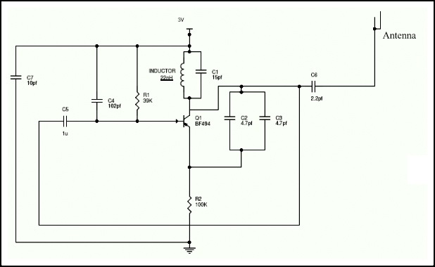 Simple Mobile Jammer Circuit Diagram
Cell Phone Jammer Circuit Explanation:
- If you understand the above circuit, this circuit analysis
is simple and easy. For any jammer circuit, remember that there are
three main important circuits. When they are combined together, the
output of that circuit will work as a jammer. The three circuits are
- RF amplifier.
- Voltage controlled oscillator.
- Tuning circuit.
- So the transistor Q1, capacitors C4 & C5 and resistor R1 constitute the RF amplifier circuit. This will amplify the signal generated by the tuned circuit. The amplification signal is given to the antenna through C6 capacitor. Capacitor C6 will remove the DC and allow only the AC signal which is transmitted in the air.
- When the transistor Q1 is turned ON, the tuned circuit at the collector will get turned ON. The tuned circuit consists of capacitor C1 and inductor L1. This tuned circuit will act as an oscillator with zero resistance.
- This oscillator or tuned circuit will produce the very high frequency with minimum damping. The both inductor and capacitor of tuned circuit will oscillate at its resonating frequency.
- The tuned circuit operation is very simple and easy to understand. When the circuit gets ON, the voltage is stored by the capacitor according to its capacity. The main function of capacitor is to store electric energy. Once the capacitor is completely charged, it will allow the charge to flow through inductor. We know that inductor is used to store magnetic energy. When the current is flowing across the inductor, it will store the magnetic energy by this voltage across the capacitor and will get decreased, at some point complete magnetic energy is stored by inductor and the charge or voltage across the capacitor will be zero. The magnetic charge through the inductor will decreased and the current will charge the capacitor in opposite or reverse polarity manner. Again after some period of time, capacitor will get completely charged and magnetic energy across the inductor will be completely zero. Again the capacitor will give charge to the inductor and becomes zero. After some time, inductor will give charge to capacitor and become zero and they will oscillate and generate the frequency.
- This circle run upto the internal resistance is generated and oscillations will get stop. RF amplifier feed is given through the capacitor C5 to the collector terminal before C6 for gain or like a boost signal to the tuned circuit signal. The capacitors C2 and C3 are used for generating the noise for the frequency generated by the tuned circuit. Capacitors C2 and C3 will generate the electronic pulses in some random fashion (technically called noise).
- The feedback back or boost given by the RF amplifier, frequency generated by the tuned circuit, the noise signal generated by the capacitors C2 and C3 will be combined, amplified and transmitted to the air.
- Cell phone works at the frequency of 450 MHz frequency. To block this 450MHz frequency, we also need to generate 450Mhz frequency with some noise which will act as simple blocking signal, because cell phone receiver will not be able to understand to which signal it has been received. By this, we can able to block the cell phone signal from reaching the cell phones.
- So here in the above circuit, we generated the 450 MHz frequency to block the actual cell phone signal. That’s what the above circuit will act as a jammer for blocking the actual signal.
- This circuit will work in the range of 100 meters i.e. it can block the signals of cell phones with in 100 meters radius.
- Usage of this type of circuits is banned in most of the countries. Usage of this circuit is illegal and if you caught by using this circuit, you can be imprisoned and also should pay large amount in the form of fine.
- This circuit can be used in TV transmission and also for remote controlled toys or play things.
- If the circuit is not working, just increase the resistor and capacitors values in the circuit. Increase the frequency of tuned circuit by using this formula F= 1/ (2*pi*sqrt (L*C)). Increase the inductor capacitor circuit components value for increasing the frequency.
contact:
DEV HARSHA
whatsapp,hike nd calls
8978511693 & 9505630317
Comments
mobile signal Jammer