We know that bugger is a device which
gives the information of one person to other person in the remote
location. Normally bugger is used for finding out the status of the
person like where he is going, what he is talking etc. This is illegal
but most of spy agencies use this bugger. Here is small circuit with which you can listen to another people conversation from long distance
using the normal FM radio set. This FM bugger circuit is kept in room
where you want listen the conversation. You can listen to this
conversation using the normal FM radio set.
FM Bugger Block Diagram:
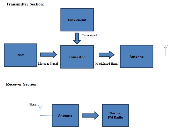
From the block diagram
we can easily understand that the message signal or conversation signal
is modulated with the carrier frequency which is generated by the tank circuit.
The message signal and carrier signal is modulated by the transistor
and transmit the modulated signal in the air through the antenna. The
modulated signal is received by the receiver antenna and gives to the FM
radio where the user can listen to the conversation. User should adjust
the receiver frequency in the radio for receiving the signal from the
transmitter.
FM Bugger Circuit Diagram:

FM Bugger Circuit Explanation:
- The circuit uses analogue modulation in which the carrier signal is applied continuously to the message signal. Here, in our circuit, the conversation of people is received by the MIC and give to the circuit is modulated to the carrier signal and transmitted.
- There are different types of analogue modulation in which one type of modulation is amplitude modulation, in which single side band (SSB) modulation and double side band modulation will come and another type of modulation is angular modulation in which the frequency modulation, phase modulation will come. In this circuit FM modulation is used. In FM modulation, frequency of the carrier signal is varied in accordance to the instantaneous amplitude of the modulating signal. Normal FM radio will use this type of modulation to transmit there signals, frequency modulation will give high throughput and efficiency when compared to amplitude modulation.
- MIC is placed in the room in which you want to listen to the conversation of the people and MIC will decode the conversation in to the signal which is given to the capacitor C1 where C1 is used for removing the noise in and turn on the transistor.
- The tank circuit (capacitor C6 and L1) which produce the carrier signal for the conversation or message signal, the transistor will amplify the both the signals and send to air through the antenna. The capacitor C4 is used to remove the noise in the transmitted signal.
- The capacitor C6 is variable because you can adjust the capacitor for producing your own carrier signal. Remember carrier signal should be in range of 88 to 105 MHz so that FM radio receiver set can receive your transmitted signal.
- The FM radio receiver set is adjusted your frequency for listening to the conversation.
Note:
- You can make L1 using about 25cm length of 25SWG wire. Wrap the wire around a cylindrical object of 6mm diameter and take it out after eight turns.
- The transmission area range is around 100 meters.
- Check whether the oscillator circuit is working properly or not before transmitting.
- You can use a dipole antenna for transmitting the signal to increase the range of the transmitter.
- Circuit operating voltage is around 3V, you can use a battery of 3V or normal DC supply as the power supply.
- For better working use the PCB board for soldering or connecting the components in the circuit.
- This circuit can be used in offices, colleges or any where you want remember bugging is illegal.
contact:
DEV HARSHA
whatsapp,hike nd calls
8978511693 & 9505630317
Comments