Multivibrator:
Multivibrator discover their own space
in lots of applications as they are among the most broadly used
circuits. The application can be anyone either a household application
or industrial or communication, etc. The multivibrator can also work in
such type of application either as an oscillator or digital flip flop or pulse generator circuit or like a timer or I can be lay generator circuit and lots more.
There are mainly three types of Multivibrators. They are
- Astable Multivibrator: It has actually no stable state. It has two quasi steady state which rapidly alters from one to another and again to the same state. So it’s mainly alters from high to low and from low to high devoid of any input trigger input after pre settled time.
- Monostable multivibrator: Out of two states, one is stable state and another one is quasi state. When trigger input is given, it switches from a stable state of quasi state. And it automatically switches to a stable state from quasi state after a pre decided time.
- Bistable Multivibrator: Both the state is stable in it. To alter the state between low and high two different input trigger is used.
555 Timer as Multivibrator to understand more about 555 timer.
All the above three types of
multivibrators can be easily constructed with the help of transistors.
But there is one type of IC which is easily obtainable that can be used
as Astable, Monostable or Bistable multivibrator and it is known as
IC555.
IC555 Pin Diagram:
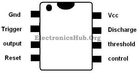
IC555 Pin Diagram
Pin Functionality of IC555:
| Provides ground | |||
| Trigger comparator input pin. Negative trigger (< 1/3 Vcc) is given in monostable operation | |||
| Its output pin | |||
| Internal flip flop reset pin. Necessity be high to enable output | |||
| Control voltage input to manage charging discharging of external capacitor | |||
| Threshold comparator input pin. Positive trigger (>2/3 Vcc) is given in bistable operation | |||
| Discharge pin. Gives discharge path to external capacitor | |||
| For +Ve biasing voltage. Between 4.5 V to 16 V |
IC 555 is one of most versatile chips
and due to its multi-functionality, it can be used in almost all kinds
of applications. It is a DIP or SOP package kind of chip having 8 pins
with direct current drive output of 200 mA. This IC is made up of analog
as well as digital components that’s why it is known as mixed signal chips. The general application of the IC is to generate timing, clock waveform, square wave oscillator and many more.
Internal Block Diagram of IC555:
Ads not by this site
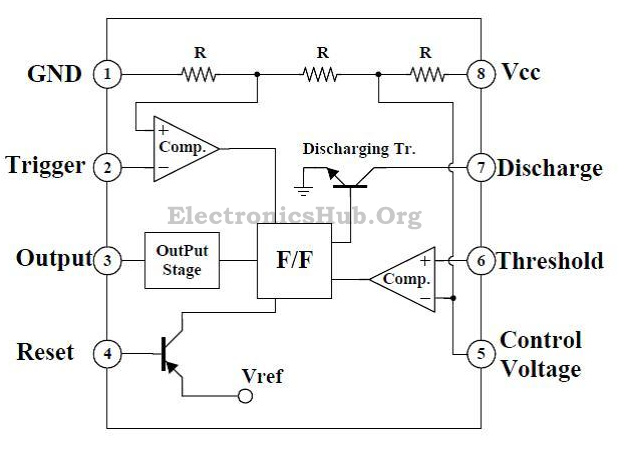
Internal Block Diagram of IC 555
As you can find in the figure above that
IC55 comprises of two comparators one is known as RS flip flop another
one is the combination of the some discrete components viz transistor,
resistor and more. The voltage for biasing is parted among three parts
by voltage divider having similar value of resistor R through these
non-inverting voltage get 1/3 Vcc of the trigger while the inverting
terminal get 2/3 Vcc of threshold comparator. R and S input terminal of
the flip flop receives the both comparator output. The real output of
the IC is Q’(Q bar) output while output terminal Q. The discharging
transistor that gives discharging way to external capacitor at the time
it reaches high.
At the time 1/3 Vcc > negative
trigger is given at the input pin trigger, the trigger comparator move
to high output and the flip flop reach to original sate and the chip
output which is output from Q’ moves to high.
Now when 2/3 Vcc < positive trigger
is given to threshold input pin, the flip flop is in set state as the
output from the threshold comparator is high. The chip output moves to
low as the output Q will turn to high. The external capacitor that
receives the discharging path during the time of transistor discharges.
The high input resets hold the flip flop to enable. At the phase of low
state flip flop put out of action and receives low at the output. No
other result of threshold as well as trigger comparator outputs.
Circuit Diagram of Police Siren Circuit using NE555 Timer:
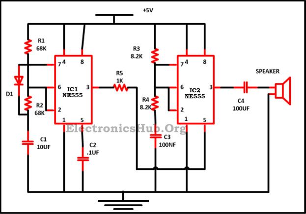
Police Siren using NE555 Timer Circuit Diagram
Description:
This circuit produces a sound similar to
the police siren. The two 555 act as an astable multivibrator. The 555
timer IC is an integrated circuit used in a variety of timer, pulse
generation and oscillator applications. The 555 can be used to provide
time delays, as an oscillator, and as a flip-flop element.In the
beginning 555 is coupled like a low-frequency oscillator so to command
the voltage at the second 555 IC at pin 5 which is a control pin.The
shifting of the voltage on pin5 is the root of the second oscillator
frequency to get up and down.
Police siren circuit which is explained here is worked on NE555 timer IC.
The circuit is build with the help of two NE555 IC(i.e. IC1 andIC2)
which is the basic block of this circuit. Both the timer IC in these
circuit is connected like a astable multivibrator. Although both the IC
in the circuit work at two dissimilar frequency.IC1 is a astable
multivibrator of slow frequency work on frequency of 20HZ and having 50%
of duty cycle while IC2 is a fast astable multivibrator works on
frequency of 600Hz. IC1 output is then serve to IC2 at the control
pin(oin5). Through the help of this arrangement IC2 output frequency
will be modulated with the IC1output frequency. The circuit works on the
DC supply between a range of 6V to 15V.
The frequency range of the siren can
vary with the exchange of R2 and R4 resistor with potentiometer. The
pitch of sound can be enlarged with the attachment of the power
amplifier at the output point. The accurate effect of police siren can
be produced by connecting flashing LEDs at the correct place. The
circuit can be made on a Perfboard. NE556 can be used in the place of
two NE555.
contact:
DEV HARSHA
whatsapp,hike nd calls
8978511693 & 9505630317
contact:
DEV HARSHA
whatsapp,hike nd calls
8978511693 & 9505630317
Comments