Summary:
This easy circuit complies 9 LED attached like a “knight rider
scanner mode”. This circuit can employ in the front side of a car. It
will present an eye catching look as the LED initially travel in the one
way and then travel reverse in the similar direction. It means same as a
pendulum it travels back and forth.
This circuit can be utilized for the beautification of the car or it
can be helpful at the time of crisis when your car broke down and you
need help.
Related Post: LED Christmas Lights Circuit
Circuit Diagram of LED Knight Rider Circuit Diagram:

LED Running Lights – LED Knight Rider Circuit Diagram
Description:
In order to get familiar with the
working layout of the circuit it is important to get familiar with
individual pin. This IC has 16 pins out of which 3 are input pin, 10 is
for output purpose and for ground one pin is assigned and one power supply and rest one left is for Carry out. As shown below pin diagram of IC CD4017.
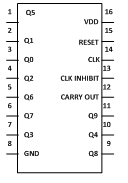 1. Input Pin:
- Reset Pin (Pin 15) – The counter is reset to zero by this pin. Suppose you wish that the counter starts counting from the third pin then you need to attached fourth output with 15 pin. So after each third output the counting automatically begins with zero.
- Clock Pin (Pin 14) – The output will be provided each time the pin 14 of the IC move to high. Like for the initial pulse of the clock pin 3 will give you output likewise for the next clock pulse arrive the output will be provided by pin2 and so on. After 10 clock pulse it will once more begins from Q0 output.
- Clock Inhibit Pin (Pin 13) – This pin is used to change the state of the counter from ON to OFF and vice versa. Pin 13 should reach the highest state if you wish to switch off the counter. If it is at high state then it will not pay attention on the clock pulse no issues that you press the switch how many of times, implies that the count will not go forward. Pin 13 in our circuit is grounded.
2. Output Pin (Pin Q0 – Q9)
– In the sequential manner the output is received from these pins. Like
pin 3 will give you output for the first pulse and so on.
3. Ground Pin (Pin 8) and Supply Pin (Pin 16) – For the working of the IC pin 8 provide ground while power supply is provided by pin16.
4. Carryout Pin (Pin 12)
– With the help of this pin one or more than one IC CD4017 can linked.
Suppose you desire to attaché one more CD4017 then attach pin 12 with
input clock of its descendant. The carry pin of primary CD4017 is
coupled with the second clock input similarly the second carry pin is
coupled with the third clock input and so on. You can see this in
circuit diagram.
NE555 and CD4017 are the two IC on which
the circuit is based along with some other components. In this circuit
IC 555 timer is used like an astable oscillator.
IC CD4017 is used as a CMOS
counter/driver. Every time when it gets to clock pulse , it fetches the
clock pulse through clock input and all 10 outputs turn on in sequence.
It is well known IC and it is very much useful in various other projects
viz Light Chaser, Matrix Die.
IC NE555 in this circuit is used as an
astable mode , used to produce a clock pulse for the circuit. This is
used to give an oscillating waveto pin 3 of the IC1 which is for
output. By the help of VR1 the speed of oscillation can be alter. 555
timer oscillation frequency can be calculated by-
f=1. 44/(R1+2* (VR1) *C1)
In this circuit, the counting will start
from 0 till 16 since we have employed two decade counters. IC2 in the
circuit done the counting 0 to 9 while with the help of diodes the rest
of the counting will done by IC3.
In the instance when 555 timer gets the
power supply, pin 3 of IC1 output is given to CD4017 pin 14 of decade
count, which in turn give clock pulse for the IC2 working. CD4017 begins
its counter value from zero (since it has inbuilt counter) after
getting the clock input. And after pin 14 moves to high it forwarded one
by one to every pin. Like at the primary stage output Q0 will receive
at pin 3 and LED1 will blink and LED2 will glow from pin4 and so on.
When the counter arrives at the pin 11
i.e ninth output it will create it temporary high, which is coupled to
pin 13 (clock inhibit). The clock pulse will be disregarded from pin 14
if the pin is at high and the counting stop by IC2.
And in return of these IC3 pin 15 became
low because earlier transistor BC547 is a high state. And pin15 of IC3
reset to low state due to this low signal for a short moment and the
output of IC3 stats counter from Q0 (pin3) and move forward one by one.
When it arrives at Q8 which is pin 9 which is yet again connected with
pin13 of IC3 due to stop counting of IC3 irrespective of the input
signal. Pin 14 disregard the clock pulse if pin13 is at high which
implies IC3 stop counting.
And this will once more given to reset
pin 15 of IC2 and counting is now begin by IC2, counting of IC3
disabled. It also means that when the output counting is done by IC2
from IC3 is stop similarly IC2 stop when IC3 counts. Hence output
signals approaching from IC3 are transmitted in reverse direction to
IC2.
Components Required for the Circuit:
- IC
- NE555 – 1
- CD4017 – 2
- Resistor
- R1 (1K) – 1
- R2 (100K) – 1
- R3 (10K) – 1
- VR1 (100K) – 1
- C2, C1 (.1uf) – 2
- D1-D9 (1N4148) – 9
- Transistor (BC547) – 1
- LED1-LED9 – 9
contact:
DEV HARSHA
whatsapp,hike nd calls
8978511693 & 9505630317
Comments