Generally appliances that we used in our
home are being controlled with the help of devices like switches,
senors. However sometimes it is dangerous to have physical contact with
these switches. So to overcome these dangers, here we have explained a
circuit that needs no physical contact with the appliance. In these
circuits all you need is to pass your hand above LDR. As you first
pass your hand over LDR the device connected with it started and remain
in that state till you again pass your hand above LDR.
 Wireless Switch Circuit – ElectronicsHub.Org
cell : 7569146411,
email:devaharsha143@gmail.com
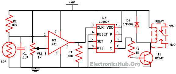
These circuits are mainly depending on
two ICs. First one is LM714 which is an operational amplifier. These IC
is used to increase the voltage level at the output hundred of a
thousand times as compared with the input. Another one is most
generally used JK flip flop i.e. CD4027. These IC works in toggle mode
and based on the JK flip flop master slave concept. This IC is used to
alter the state when the signal is given to the any one of the input
terminals and can get more than single output. There are four input
pins in JK flip flop named J and K along with set and reset pin and Q
and Q¯ for output.
 Wireless Switch Circuit – ElectronicsHub.Org
Description:
The circuit is made up of Operational
amplifier LM741 which is employed like a comparator for sensitive
voltage, LDR , Preset VR1 is used to give a reference voltage to the pin
3 which is a non-inverting terminal as well as to LDR and R2 is linked
with IC1 at inverting pin 2 along with a few additional components.
It is very simple to understand the
working of the circuit. LDR device will not start till we do not pass
our hand over it and as a result of it IC1 pin 2 move to high state. And
as a result of its low state is achieved by the IC1 pin 6 which is an
output pin.
Now as soon as someone passes their
hand over LDR, IC1 pin 3 is set to high as compared with the IC1 pin 2
as a result of its pin 6 reaches to high state which supply a clock
pulse to 13 pins of IC2 (a flip flop IC). The logic level present at the
input terminal ie. J and K guarded the state of a flip flop with the
help of some internal control. With the positive going cycle of the
clock changes occur. Set and Reset pin are not dependant on the clock
and it started when high signal is provided to any one of the input
pins.
The circuit revealed is triggered on the
primary rim of the switch pulse ie output vary when you once more place
your hand above LDR. As in the circuit you can find that J and K both
attached to high input which implies that at each transition of the
clock pulse whether negative or positive pin 13 fluctuate between high
and low. This can be demonstrated with the assist of JK flip flop truth
table. Hence when it got the pulse from clock from IC1 as of hand above
LDR transistor attached to pin 15 begins condition and the output is
get with the help of relay attached in the circuit. With the help of
the VR1 sensitivity of LDR can be adjusted.
Components used in this Circuit:
- IC
- CD4027 – 1
- LM741 – 1
- Resistor
- R1 (1K) – 1
- R2 (82K) – 1
- R3 (10K) – 1
- VR1 (5K) – 1
- Relay – 1
- D1 (1N4007) – 1
- LDR – 1
- T1 (BC547) – 1
- C (. 1uF) – 1uit
cell : 7569146411,
email:devaharsha143@gmail.com
Comments